PXIe-148X Getting Started Example - Common Generation Tutorials
This document covers a range of common scenarios using the PXIe-148X Generation Getting Started Example (GSE) to help you understand LLP generation, I2C and GPIO timestamping, and common configuration options.
Note: This document references the example included with the NI-FlexRIO 22Q3 driver. Examples included in newer releases of the driver should be applicable.
Table of contents
- PXIe-148X Getting Started Example - Common Generation Tutorials
Prerequisites
This tutorial is written for users who understand how to perform a basic generation and a basic acquisition with PXIe-148X GMSL or FPD-Link interface modules. It is recommended to complete the PXIe-148X Getting Started Example - Basic Acquisition Tutorial and PXIe-148X Getting Started Example - Basic Generation Tutorial before attempting this tutorial.
Note: The tutorials in this document assume the use of a PXIe-148X GMSL or FPD-Link Generation Interface module and an Acquisition Interface module connected to SI0 and SO0 of the respective modules. A Leopard Imaging IMX490 camera is also used to acquire packet data and replay it through a generation interface module. See PXIe-148X Getting Started Example - Basic Acquisition Tutorial and Basic Generation Tutorial for specific setup if needed.
Generation and Acquisition Topics
This tutorial expects that SO0 of a generation module and SI0 of an acquisition module are cabled together. This tutorial uses one generation LabVIEW project and one acquisition LabVIEW project to demonstrate the generation capabilities of the generation module.
Note: For the purposes of this tutorial, all input control values not specified should be left with their default values.
Performing a Simple Generation and Acquisition
- Create a TDMS file for generation. There are two options for creating a TDMS file:
| Option | Description |
|---|---|
| Option A: Create a TDMS file | Double click the Create CSI-2 Packet TDMS Files VI in the generation LabVIEW project and create a TDMS file for SI0. Leave all values default. |
| Option B: Acquire data from a camera | Acquire data from a camera. If the data was acquired from a camera attached to a serial input channel other than SI0, rename the TDMS file on disk to have SI0 in the name to generate on SI0. Copy the acquired TDMS file to the default TDMS folder for generation. |
-
Double-click the Generation Example VI in the LabVIEW project.
- Set the following controls on the Generation Example GSE VI and leave all other values at their defaults.
Note: VI controls and indicators can be reset to default values by clicking on the Edit menu and selecting the Reinitialize Values to Default option.
Tab Control Value Resource RIO Device [System Specific] Resource Bitfile Path Refer to Bitfile Path in the PXIe-148X Generation GSE Help -
Double-click the Acquisition Example VI in the Acquisition LabVIEW project.
- Set the following controls on the Acquisition Example GSE VI and leave all other values at their defaults.
Note: VI controls and indicators can be reset to default values by clicking on the Edit menu and selecting the Reinitialize Values to Default option.
Tab Control Value Resource RIO Device [System Specific] Resource Bitfile Path Refer to Bitfile Path in the PXIe-148X Acquisition GSE Help Serial Channel Configuration Script Refer to Configuration Script in the PXIe-148X Acquisition GSE Help -
Run the Generation Example VI and wait for the Waiting for Serializer Setup indicator to illuminate.
-
Run the Acquisition Example VI.
-
After the Acquisition Example VI indicates acquisition has started, click Serializer Setup Complete on the Generation VI before the Acquisition VI stops.
- Select the First Display Channel tab on the Acquisition Example and on the Generation Example and verify that images from the generated TDMS file are displayed on these tabs. The images should look identical.
Generating and Displaying I2C Timestamps
This section shows how to acquire and view I2C timestamps on a PXIe-148X interface module. You will use the Generation Example VI to run a script to create I2C traffic.
Note: Timestamps are relative to a time immediately after the FPGA bitfile is downloaded and run, not to the start of the acquisition. This allows for capturing I2C and GPIO timestamps during configuration, before the acquisition starts.
- Set the following controls on the Acquisition Example GSE VI and leave all other values at their defaults.
Note: VI controls and indicators can be reset to default values by clicking on the Edit menu and selecting the Reinitialize Values to Default option.
Tab Setting Value Resource RIO Device [System Specific] Resource Bitfile Path Refer to Bitfile Path in the PXIe-148X Acquisition GSE Help Resource Display Acquired Images Disabled Resource Log I2C to Disk Enabled -
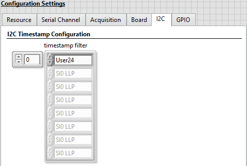
Select the I2C tab and make the following modification.
The I2C tab only has one control, the I2C timestamp filter. This filter contains an array of timestamp IDs. User24 represents the I2C traffic on serial channel 0 (SI0), User25 represents the I2C traffic on serial channel 1 (SI1), and so on.
- Set the timestamp filter array to contain only the User24 timestamp ID. This will let you see the I2C traffic on SI0. If you run the VI with a configuration script selected, you will see configuration traffic in the I2C Data Output tab after the VI has stopped.
- Set the following controls on the Generation Example GSE VI and leave all other values at their defaults.
Note: VI controls and indicators can be reset to default values by clicking on the Edit menu and selecting the Reinitialize Values to Default option.
Tab Setting Value Resource RIO Device [System Specific] Resource Bitfile Path Refer to Bitfile Path in the PXIe-148X Generation GSE Help Resource Display Generated Images Disabled Resource Log I2C to Disk Enabled Serial Channel Serializer (Output) Configuration Script Refer to Configuration Script in the PXIe-148X Acquisition GSE Help -
Select the I2C tab on the Generation VI and make the following modification.
The I2C tab only has one control, the I2C timestamp filter. This filter contains an array of timestamp IDs. User24 represents the I2C traffic on serial channel 0 (SI0), User25 represents the I2C traffic on serial channel 1 (SI1), and so on.
- Set the timestamp filter array to contain only the User24 timestamp ID. This will let you see the I2C traffic on SI0. If you run the VI with a configuration script selected, you will see configuration traffic in the I2C Data Output tab after the VI has stopped.
-
Run the Acquisition VI.
-
Run the Generation VI.
Note: Because a script was defined in the Serializer (Output) Configuration Script control, the generation begins immediately when you run the VI and does not wait for Waiting for Serializer Setup to illuminate as seen in previous sections of this tutorial. In this scenario, the Acquisition VI must be started before the Generation VI.
- Select the I2C Timestamps tab on the Generation VI to view I2C timestamp data.
-
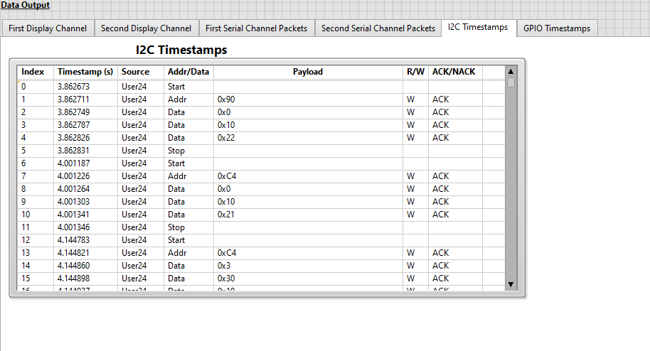
View the displayed I2C timestamp data in the I2C Timestamps table. The I2C Timestamps table displays I2C timestamp information for all I2C traffic. I2C timestamps begin logging immediately after the FPGA bitfile is downloaded and include timestamp data prior to the start of the LLP packet data acquisition (i.e. I2C traffic from the configuration script).
Note: To display I2C timestamp data, Log I2C to Disk must be enabled and the desired timestamp IDs must be added to the timestamp filter array. The displayed I2C timestamp data is read from the
User_Timestamps.tdmsfile and filtered to display only the timestamp IDs included in the timestamp filer array. The I2C Timestamps display is updated after the acquisitions completes.
-
-
Select the I2C Timestamps tab on the Acquisition VI to view I2C timestamp data.
Setting FPGA Display Parameters
You can use the FPGA Display Parameters to change the images displayed during generation.
- Set the following controls on the Generation Example GSE VI and leave all other values at their defaults.
Note: VI controls and indicators can be reset to default values by clicking on the Edit menu and selecting the Reinitialize Values to Default option.
Tab Control Value Resource RIO Device [System Specific] Resource Bitfile Path Refer to Bitfile Path in the PXIe-148X Generation GSE Help Resource TDMS File Directory A directory path to TDMS files containing LLP Packet data for serial output channels (e.g. SI0_LLP_Packets.tdms) Note: The TDMS File Directory is a folder selection and the browse dialog shows folders only, not file names.
Use the default TDMS File Directory value if you are generating from a TDMS file that was created with default settings by the Create CSI-2 Packet TDMS Files utility. See the PXIe-148X Getting Started Example - Basic Generation Tutorial for details on creating TDMS files.
Displaying Generated Images
The logic for FPGA display parameters is shared for all PXIe-148X getting started examples. Therefore, you can use the acquisition tutorial for this objective, with a few minor differences.
- Complete the steps in PXIe-148X Getting Started Example - Common Acquisition Tutorials with the following differences.
- Replace all references to SI0 with SO0.
- When running the Generation Example VI, wait for the Waiting for Serializer Setup indicator to illuminate and then click Serializer Setup Complete.
Reducing System Bandwidth Usage
The logic for FPGA display parameters is shared for all PXIe-148X getting started examples. Therefore, you can use the acquisition tutorial for this objective, with a few minor differences.
- Complete the steps in PXIe-148X Getting Started Example - Common Acquisition Tutorials with the following differences.
- When running the Generation Example VI, wait for the Waiting for Serializer Setup indicator to illuminate and then click Serializer Setup Complete.
Setting RAW Display Parameters
This section shows you how to configure the RAW Display Parameters to change the interpretation of images being displayed during generation. The logic for FPGA display parameters is shared for all PXIe-148X getting started examples. Therefore, you can use the acquisition tutorial for this objective, with a few minor differences.
Note: The effect on TDMS files of the RAW display parameter settings is different depending on whether the TDMS files are created with the Create CSI-2 Packet TDMS Files utility or contain image data acquired from a camera.
- Set the following controls on the Generation Example GSE VI and leave all other values at their defaults.
Note: VI controls and indicators can be reset to default values by clicking on the Edit menu and selecting the Reinitialize Values to Default option.
Tab Control Value Resource RIO Device [System Specific] Resource Bitfile Path Refer to Bitfile Path in the PXIe-148X Generation GSE Help Resource TDMS File Directory A directory path to TDMS files containing LLP Packet data for serial output channels (e.g. SI0_LLP_Packets.tdms) Note: The TDMS File Directory is a folder selection and the browse dialog shows folders only, not file names.
Use the default TDMS File Directory value if you are generating from a TDMS file that was created with default settings by the Create CSI-2 Packet TDMS Files utility. See the PXIe-148X Getting Started Example - Basic Generation Tutorial for details on creating TDMS files.
- Complete the steps in PXIe-148X Getting Started Example - Common Acquisition Tutorials with the following differences.
- Replace all references to SI0 with SO0.
- When running the Generation Example VI, wait for the Waiting for Serializer Setup indicator to illuminate and then click Serializer Setup Complete.
Setting Serial Channel Configurations
You can generate and display images on multiple serial output channels and set a start trigger delay with the settings on the Serial Channel tab.
Complete Creating TDMS Files to Generate Multiple Images, Generating and Displaying Multiple Images, and Setting a Start Trigger Delay in sequence in this section.
Creating TDMS Files to Generate Multiple Images
-
Open the Create CSI-2 Packet TDMS Files utility in the LabVIEW project.
-
Run the VI with all default settings to generate a TDMS file for channel SI0 that contains 10 frames at 1920 × 1080 resolution.
- Make the following modifications on the Create CSI-2 Packet TDMS Files utility front panel to generate a second TDMS file with image data differing from the first TDMS file created in the previous step.
- Set the value at index 0 of the Serial Input Channels array to SI1.
- Make the following modifications to the Frame Data Configuration control.
- Set the horizontal resolution control value to 2880.
- Set the vertical resolution control value to 1280.
The Create TDMS Files utility settings are now similar to the image below.
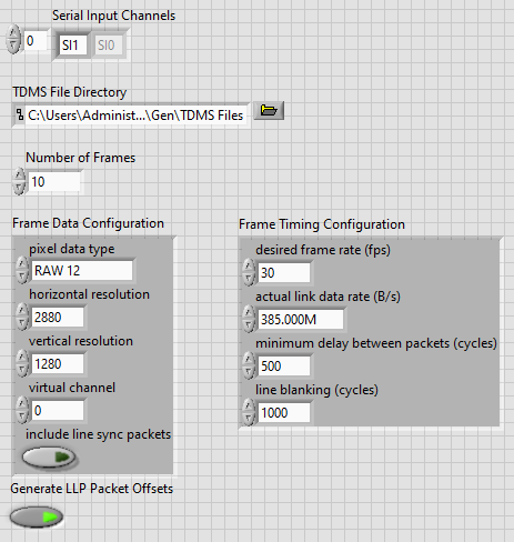
- Run the VI to generate a TDMS file for channel SI1 that contains 10 frames at 2880 × 1280 resolution.
Generating and Displaying Multiple Images
- Set the following controls on the Generation Example GSE VI and leave all other values at their defaults.
Note: VI controls and indicators can be reset to default values by clicking on the Edit menu and selecting the Reinitialize Values to Default option.
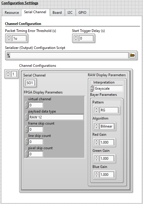
Tab Control Value Resource RIO Device [System Specific] Resource Bitfile Path Refer to Bitfile Path in the PXIe-148X Generation GSE Help - Select the Serial Channel tab and make the following modifications.
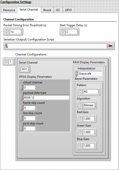
- Select index 0 of the Channel Configurations array and make the following modifications.
- Select Grayscale on the Interpretation control in the RAW Display Parameters cluster.
- Select index 1 of the Channel Configurations array and make the following modifications.
- Set the Serial Channel control value to SO1.
- Select Grayscale on the Interpretation control in the RAW Display Parameters cluster.
The settings on the Serial Channel tab are now similar to the image below.
- Select index 0 of the Channel Configurations array and make the following modifications.
- Run the VI, wait for the Waiting for Serializer Setup indicator to illuminate, and click the Serializer Setup Complete control button to start the generation.
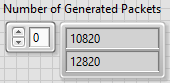
Once the generation completes, notice the Number of Generated Packets indicator array shows a value of 10820 at index 0 and 12820 at index 1, which equals the number of packets per frame (vertical resolution) times the number of frames generated for each channel. The indices in the Number of Generated Packets array correspond to the indices in the Channel Configurations array.
- Click the First Display Channel tab to view the last frame displayed for SO0.
Note that the image resolution matches the 1920x1080 resolution of the TDMS file created for SI0.
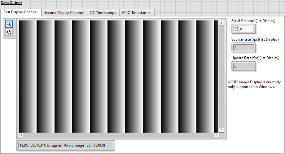
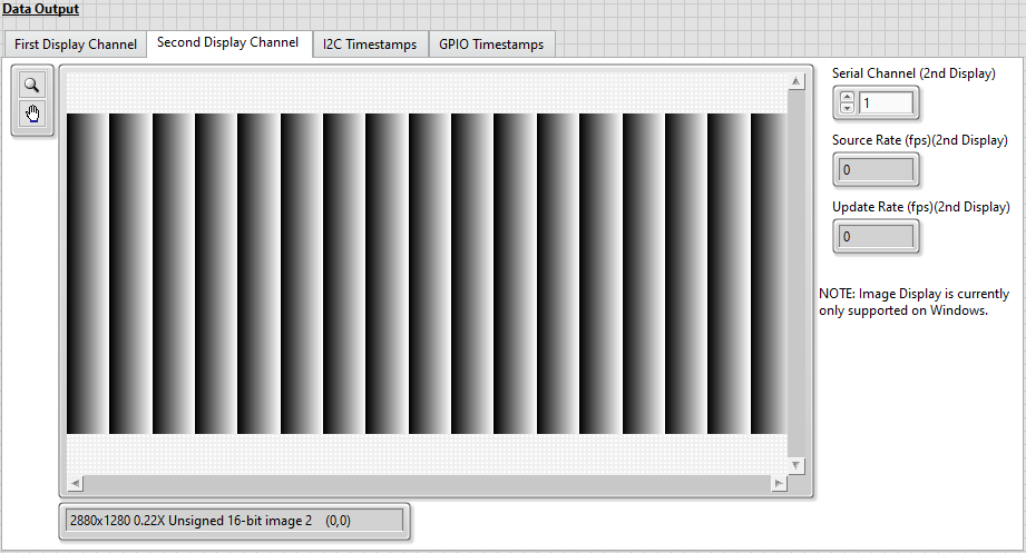
- Click the Second Display Channel tab to view the last frame displayed for SO1.
Note that the image resolution matches the 2880x1280 resolution of the TDMS file created for SI1.
Setting a Start Trigger Delay
You can use start trigger delay to delay the start of image generation. Image data acquired using the PXIe-148X Acquisition getting started example often has several seconds of delay before the first packet is acquired while the camera is configured. The PXIe-148X Generation getting started example sets a negative packet timing offset value relative to the first packet timestamp in the TDMS file to prevent any unwanted delay in the start of generation. Use the Start Trigger Delay (s) control to implement delay. Refer to the Start Trigger Delay (s) description in the PXIe-148X Generation GSE Help for additional details.
-
Select the Serial Channel tab and set the Start Trigger Delay (s) control value to 2.
The settings on the Serial Channel tab are now similar to the image below.
-
Run the VI, wait for the Waiting for Serializer Setup indicator to illuminate, and click the Serializer Setup Complete control button to start the generation.
The start of packet transmission is delayed and thus the image display is also delayed. Notice that there is now a 2 second delay before images are generated and displayed after clicking the Serializer Setup Complete button.
Using the General Purpose Input/Output (GPIO) Lines
This section shows you how to configure routing of GPIO lines between GPIO banks as well as how to manually read and write to the GPIO banks on the PXIe-148X interface module. This procedure modifies GPIO line values while the generation is running, logs the GPIO timestamps to disk, and displays digital waveforms of the GPIO lines.
Note: Timestamps are relative to a time immediately after the FPGA bitfile is downloaded and run, not to the start of the generation. This allows for capturing I2C and GPIO timestamps during configuration before the generation starts.
- Set the following controls on the Generation Example GSE VI and leave all other values at their defaults.
Note: VI controls and indicators can be reset to default values by clicking on the Edit menu and selecting the Reinitialize Values to Default option.
Tab Setting Value Resource RIO Device [System Specific] Resource Bitfile Path Refer to Bitfile Path in the PXIe-148X Generation GSE Help Resource Display Generated Images Disabled Resource Log GPIO to Disk Enabled
Creating a TDMS File for the GPIO Tutorial
-
Open the Create CSI-2 Packet TDMS Files utility in the LabVIEW project.
- Make the following modifications on the Create CSI-2 Packet TDMS Files utility front panel.
- Set the Number of Frames control to 60
- Update the Frame Data Configuration cluster with the following settings.
- Set the horizontal resolution control value to 640.
- Set the vertical resolution control value to 480.
- In the Frame Timing Configuration cluster, set the desired frame rate (fps) control to 1.
The Create TDMS Files utility settings are now similar to the image below.

- Run the VI to generate a TDMS file for channel SI0 containing 60 frames at 640 × 480 resolution.
The frame rate of 1 frame per second will cause the generation to run for 1 minute, which will allow enough time to manually read and write to GPIO during the generation.
Manually Reading and Writing to GPIO
This section shows you how to perform manual reads and writes to GPIO during generation and how to display digital waveforms for the resulting GPIO timestamp data.
Note: Complete Creating a TDMS File for the GPIO Tutorial before you begin this section.
- Select the GPIO tab and make the following modifications.
- Update the GPIO to Display array with the following settings.
- At index 0 select Ser0 GPIO in the GPIO Bank control and set the GPIO Number to 0.
Setting these values enables display of GPIO traffic for GPIO line 0 on the SO0 channel. Optionally, add any additional GPIO lines to display.
The GPIO to Display control specifies GPIO lines to display on the GPIO Timestamps Waveform after the generation completes. Timestamps for GPIO lines not included in the GPIO to Display array are logged but not displayed.
-
Select SO0 Serializer from the GPIO Bank Select drop down menu.
The GPIO Bank Select control specifies the GPIO bank used for the GPIO Bank Output, GPIO Bank Output Enable, and GPIO Bank Read controls during the generation. The GPIO Bank Select selection may be changed at runtime.
- In the GPIO Bank Output Enable cluster, enable the GPIO 0 control.
The GPIO Bank Output Enable controls are used as write enables for manual GPIO writes to override the defined GPIO routing. In this case, this option writes to line 0 of the GPIO selected on the GPIO Bank Select control and leaves all other lines in the bank unchanged.
The settings on the GPIO tab are now similar to the image below.
- Update the GPIO to Display array with the following settings.
-
Run the VI, wait for the Waiting for Serializer Setup indicator to illuminate, and click the Serializer Setup Complete control button to start the generation.
- Click Update GPIO Output to write a false value to line 0 on the SO 0 Serializer GPIO bank.
Notice that the GPIO 0 Boolean indicator in the GPIO Bank Read cluster is not illuminated (false).
- Set the GPIO 0 button in the GPIO Bank Output control to true and then click the Update GPIO Output button to write a true value to line 0 on the SO 0 Serializer GPIO bank.
Notice that the GPIO 0 Boolean indicator in the GPIO Bank Read cluster is illuminated (true).
- Set the GPIO 0 button in the GPIO Bank Output control to false and then click the Update GPIO Output button to write a false values to line 0 on the SO 0 Serializer GPIO bank.
Notice that the GPIO 0 Boolean indicators in the GPIO Bank Read cluster are not illuminated (false).
-
Click the Stop Generation button.
-
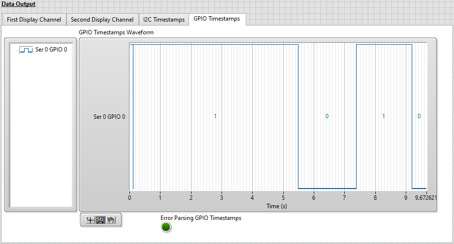
Once the VI stops running, click on the GPIO Timestamps tab to view a digital waveform of the selected GPIO line(s).
GPIO timestamp data is displayed in the GPIO Timestamps Waveform digital waveform indicator. The pattern observed matches the sequence of manual writes that were performed on GPIO line 0 during the tutorial.
Note: The digital waveform is read from the GPIO_Timestamps.tdms file and filtered to display only timestamps for the GPIO lines included in the GPIO to Display array. The GPIO Timestamps Waveform display is updated after the generation completes.
Routing GPIO Lines
This tutorial shows you how to define GPIO line routes between GPIO banks on Serial Input/Output channel pairs. A GPIO line route is the combination of a source GPIO line where data is read and of a destination GPIO line on the FPGA. Manual GPIO writes performed from the host override the GPIO routes.
Notes:
- This tutorial only applies to interface modules with both serial input and serial output channels since GPIO routing is done between pairs of input and output channels.
- Complete the Creating a TDMS File for the GPIO Tutorial section before attempting the steps in this section.
- The focus of this tutorial is on configuring GPIO routes, not manually reading and writing to GPIO or displaying digital waveforms of GPIO timestamps. For more detailed descriptions of those topics, see Manually Reading and Writing to GPIO.
- Select the GPIO tab and make the following modifications.
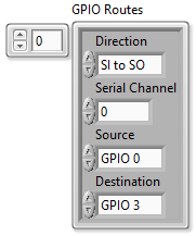
- Add a GPIO route at index 0 of the GPIO Routes array with the following settings.
- Select SI to SO in the Direction control.
- Set Serial Channel to 0.
- Select GPIO 0 in the Source control.
- Select GPIO 3 in the Destination control.
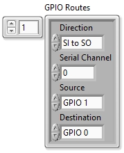
- Add a GPIO route at index 1 of the GPIO Routes array with the following settings.
- Select SI to SO in the Direction control.
- Set Serial Channel to 0.
- Select GPIO 1 in the Source control.
- Select GPIO 0 in the Destination control.
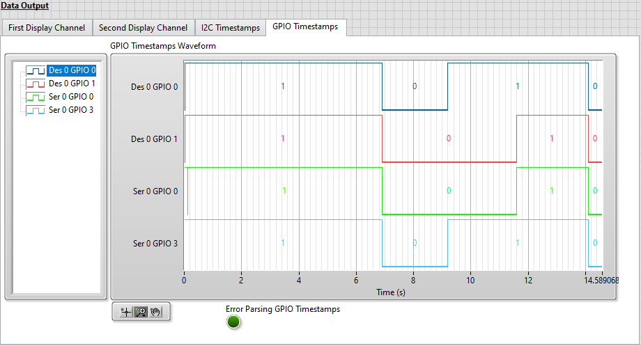
These settings define the GPIO routes shown below.
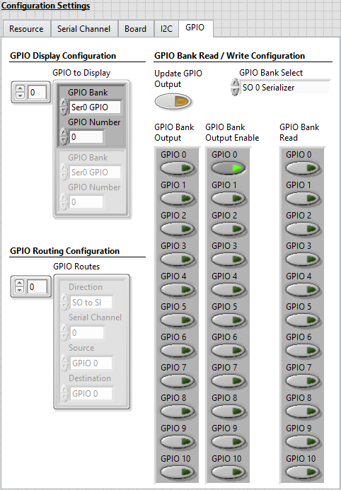
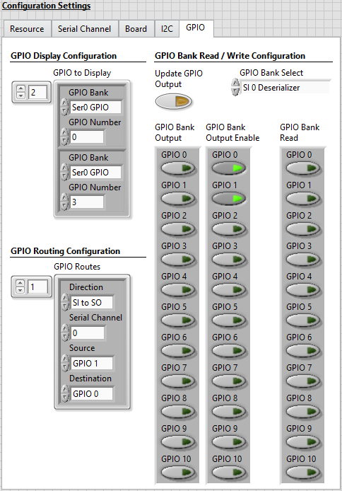
From (Source) To (Destination) SI 0 Deserializer Line 0 SO 0 Serializer Line 3 SI 0 Deserializer Line 1 SO 0 Serializer Line 0 - Update the GPIO to Display array with the following settings.
- At index 0, select Des0 GPIO in the GPIO Bank control and set the GPIO Number to 0.
- At index 1, select Des0 GPIO in the GPIO Bank control and set the GPIO Number to 1.
- At index 2, select Ser0 GPIO in the GPIO Bank control and set the GPIO Number to 0.
- At index 3, select Ser0 GPIO in the GPIO Bank control and set the GPIO Number to 3.
-
Select SI 0 Deserializer from the GPIO Bank Select drop down menu.
- In the GPIO Bank Output Enable cluster, enable the GPIO 0 and GPIO 1 controls.
The settings on the GPIO tab are now similar to the image below.
- Add a GPIO route at index 0 of the GPIO Routes array with the following settings.
-
Run the VI, wait for the Waiting for Serializer Setup indicator to illuminate, and click the Serializer Setup Complete control button to start the generation.
-
Click Update GPIO Output to write false values to lines 0 and 1 on the SI 0 Deserializer GPIO bank.
-
Set the GPIO 0 button in the GPIO Bank Output control to true (illuminated) and then click the Update GPIO Output button to write a true value to line 0 on the SI 0 Deserializer GPIO bank.
-
Set the GPIO 1 button in the GPIO Bank Output control to true and then click the Update GPIO Output button to write a true value to line 1 on the SI 0 Deserializer GPIO bank.
-
Set the GPIO 0 and GPIO 1 buttons in the GPIO Bank Output control to false and then click the Update GPIO Output button to write false values to lines 0 and 1 on the SI 0 Deserializer GPIO bank.
-
Click the Stop Generation button.
-
Once the VI stops running, click on the GPIO Timestamps tab to view a digital waveform of the selected GPIO lines.
GPIO timestamp data is displayed in the GPIO Timestamps Waveform digital waveform indicator. The waveforms observed are for the sources and the destinations of the defined GPIO routes. Notice that the values written to the source GPIO lines match the values read on the destination GPIO lines.